Inside the Memory Hierarchy and Model of AMD CDNA GPUs
Introduction
Modern GPUs are designed to maximise throughput over latency. Many concurrent execution units and thousands of threads running simultaneously make even small synchronization costs a scalability bottleneck. As a result, GPU architectures avoid enforcing strong, implicit ordering guarantees and instead expose weaker memory models that allow hardware to make progress without unnecessary coordination.
The responsibility of enabling synchronization and enforcing visibility is shifted to the software. This increases the complexity for programmers and compiler backends but enables the hardware to sustain high throughput at scale.
This post focuses on cache organization, cache policies, memory visibility, synchronization mechanisms and the constraints that shape these choices. The goal is to reason about why these mechanisms exist and how the compiler backend leverages them to allow synchronization.
Overview of CDNA-4 Architecture
GPUs are designed around massive parallelism and high throughput rather than low-latency single-thread execution. In line with this design philosophy, CDNA 4 GPUs consist of many execution domains known as Compute Units (CUs). Each compute unit is composed of vector and matrix execution pipelines, scalar control logic, and dedicated hardware for issuing and tracking memory operations.
More importantly, each compute unit contains private on-die SRAM structures that serve as a per-CU L1 cache, as well as a distinct on-die SRAM region used for software-managed shared memory, referred to as the Local Data Share (LDS) in AMD terminology. This differs from NVIDIA’s approach, where the L1 cache and shared memory reside in the same SRAM and their sizes are configurable.
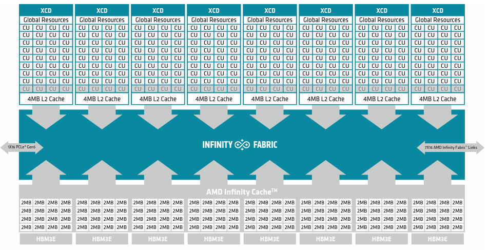
32 (varies between CDNA-3 and CDNA-4) Compute Units are resident inside one Accelerator Complex Die (XCD) in CDNA-4. Each XCD contains a second level of cache (L2 Cache) which is shared by all the Compute Units inside it. The entire GPU consists of 8 such XCDs in total.
The XCDs are interconnected by AMD’s Infinity Fabric. AMD’s Infinity Fabric provides coherent memory access across the system, which spans multiple chips.
There is an additional third level cache (L3) called the Infinity cache. It is a Memory Side Cache (More on this later) and its primary purpose is to reduce the latency of HBM access.
Too Many Caches for Coherence
Modern CPUs provide cache coherence by default: the private L1 cache of each core participates in a hardware coherence protocol, ensuring that writes performed by one core are observed by others. This approach scales well for CPUs, which typically consist of a few to a few dozen cores.
GPUs, however, operate at a radically different scale. A CDNA-4 GPU contains hundreds of compute units, each backed by a private L1 cache. This necessitates a radically different approach to cache design. For example, maintaining coherency at L1 cache level is infeasible due to the hardware resources and bandwidth it would consume. To understand GPU cache design, we now examine the GPU cache hierarchy through the lens of the AMD CDNA architecture.
With respect to L1 caches, CDNA-4 has three separate L1 caches serving different memory accesses.
- Vector L1 Cache : Memory accesses from Vector Memory operations.
- Scalar L1 Cache : Memory accesses from Scalar Memory operations.
- Instruction L1 Cache : Caches instructions
The most important of these is the Vector L1 cache as it handles most of the memory accesses in the workload. The scalar L1 cache is typically used for loading constants (Base Address etc) and the instruction cache is Read-Only by design.
One Vector L1 cache is present per compute unit. However, one Instruction L1 cache is shared by two compute units because there tends to be an overlap between the instructions being executed by wavefronts (warps) in different compute units. Similarly, the Scalar L1 cache is shared by multiple compute units as well. From this point forward, we will refer to the Vector L1 cache as simply the L1 cache.
The L1 cache is designed as a write-through cache. This choice simplifies the hardware by eliminating the need for per-line dirty state, ownership tracking, or participation in coherence protocols with other Compute Units.
L1 caches are non-coherent, meaning that different compute units may hold independent and potentially stale copies of the same cache line. This is an important point because it affects memory synchronization between wavefronts (warps in NVIDIA's terminology) executing on different Compute Units. There is also a TA Unit which is part of the L1 cache. The primary purpose of the TA unit is to coalesce memory accesses to minimize the number of L1 cache accesses and write-throughs to L2 performed.
L2 cache (4 MB) is designed to be the point of coherency. It is a write-back and write-allocate cache that serves an entire XCD. The L2 is coherent within an XCD and Coherence among L2 caches of different XCDs is maintained with the help of snoop filters present in the data fabric. Global Memory Atomic operations execute directly in the L2 cache (bypassing L1 cache entirely)
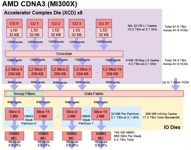
The Infinity Cache is a large (256 MB) memory-side cache that sits on the path between the on-die caches and HBM. Because it is attached directly to the memory controllers, all DRAM traffic is routed through it. Unlike the L1 and L2 caches, the Infinity Cache does not participate in coherence and never holds dirty data. Its sole role is to cache clean memory lines to reduce the effective latency and bandwidth pressure of HBM accesses.
From the AMD CDNA-3 Whitepaper
The AMD Infinity Cache was carefully designed as a shared memory-side cache, meaning that it caches the contents of memory and cannot hold dirty data evicted from a lower level cache. This has two significant benefits. First, the AMD Infinity Cache doesn’t participate in coherency and does not have to absorb or handle any snoop traffic, which significantly improves efficiency and reduces the latency of snooping from lower level caches. Second, it can actually hold nominally uncacheable memory such as buffers for I/O.
Shared Memory
In addition to the cache hierarchy, each compute unit contains a low-latency on-die SRAM region, referred to as the Local Data Share (LDS), that serves as shared memory for all wavefronts executing on that compute unit. Unlike vector memory accesses, which flow through the vector memory pipeline and its associated caches, LDS provides a software-managed storage space with explicit visibility to all wavefronts resident on the same compute unit.
However, LDS also introduces an orthogonal class of memory operations that must be explicitly synchronized. Memory instructions issued to different pipelines are not globally ordered with respect to one another. For example, a wavefront issuing a load from LDS and a load from global memory has no architectural guarantee as to which operation will complete first. Similarly, if wavefront A issues a store to LDS and wavefront B subsequently issues a load from the same address, the architecture provides no guarantee that B will observe A’s write unless explicit synchronization is performed.
On CDNA-3, the size of the shared memory is 64 KB while in CDNA-4 this was increased to 160 KB. The LDS is banked (32 Banks on CDNA-3, each bank is 4 bytes wide). Each bank can be accessed independently in the same clock cycle giving a throughput of 128 bytes/cycle.
Note: Bank Conflicts and Address Swizzling
Shared memory (LDS) is internally divided into multiple banks to allow parallel access by wavefront lanes. If multiple lanes access addresses that map to the same bank, the accesses are serialized, reducing effective throughput.
To mitigate this, GPU architectures employ address swizzling, a layout transformation that distributes adjacent data across different banks. By reshaping the physical address mapping, swizzling reduces the likelihood of bank conflicts when wavefronts access contiguous or strided data patterns.
LDS also contains atomic execution units which allow the GPU to perform atomic operations directly within the LDS.
Note: LDS and Occupancy
The size of the Local Data Share (LDS) is one of the key factors (the other being register pressure) in determining the maximum achievable occupancy of a compute unit. Because LDS is allocated per kernel instance on a CU, larger per-workgroup LDS requirements directly limit how many wavefronts can be resident concurrently.
The transition from CDNA 3 to CDNA 4 increased the available LDS capacity per compute unit, partially alleviating this constraint and enabling higher potential occupancy for LDS-intensive kernels. In addition to its role in occupancy, the low access latency of LDS allows more data to be staged close to the execution pipelines. This helps keep vector and matrix units fully utilized.
With this hierarchy in mind, we can now reason about how visibility and ordering are defined on CDNA GPUs.
Memory Ordering and Visibility
Now that we have covered all the essentials about memory hierarchy, we can talk about Memory Model on AMD GPUs. GPUs implement a weak memory model which allows them to maximize throughput and avoid synchronization overhead unless explicitly requested for.
On AMD CDNA GPUs, there are broadly three distinct types of memory operations.
- Vector Memory Operations : Loading/Storing data from global memory to VGPRs (Registers specific to each thread)
- Scalar Memory Operations : Loading/Storing data from global memory to SGPRs (Registers common to all 64 threads in a wavefront)
- LDS Memory Operations : Loading/Storing data from shared memory
We will focus on the Vector Memory and the LDS Memory operations as they are more important in most workloads.
Scope and Reuse Hint
The L1 cache associated with a compute unit is non-coherent. As a result, cache lines are not automatically invalidated when the same address is written by a wavefront executing on a different compute unit. Without additional mechanisms, a wavefront could repeatedly observe a stale value that resides in its private L1 cache.
One way to avoid this would be to invalidate the entire L1 cache before performing such a load, thereby forcing the access to be serviced by the next cache level. However, indiscriminately invalidating L1 on every access would be prohibitively expensive and would negate most of the performance benefits of having a private cache.
To address this, every vector memory operation on CDNA GPUs explicitly specifies a scope, which defines the visibility requirements of the operation and, by extension, the cache levels that may be consulted. The architecture defines four valid scope values:
- Wave: The memory load/store operation is visible to all 64 threads in a wave
- Group: The memory load/store operation is visible to all threads in the same Workgroup
- Agent/Device: The memory load/store operation is visible across the entire GPU
- System: The memory load/store operation is visible across the entire system where system can be CPU + GPU or multiple GPUs
These scope bits dictate cache policy at each level of the cache. Additionally, a Non-Temporal bit indicates whether to expect temporal reuse for the data or not. In general, if this bit is set, the relevant cache line is evicted because it is unlikely to be reused again.
For a memory operation with a given scope, the architecture must ensure that the operation does not observe data from any cache level whose contents are not guaranteed to be coherent at that scope. As a result, the cache hierarchy may be selectively bypassed/invalidated depending on where coherence is enforced for that scope.
For example, a memory load with group scope is allowed to hit in the L1 cache, because all wavefronts within a workgroup execute on the same Compute Unit and therefore share the same L1. In contrast, a memory load with device scope must bypass the L1 cache and, in configurations with more than one L2 cache per agent, must also bypass L2. This ensures that the load observes a value that is coherent at device scope, even if the most recent store was performed by a wavefront executing on a different XCD.
The ISA details the behaviour for each scope as below -
Table 1: Load Control Behaviors
| Scope | SC1 | SC0 | NT | CU Cache Behavior | L2 Cache Behavior | Last-level Cache Behavior |
|---|---|---|---|---|---|---|
| Wave | 0 | 0 | 0 | Hit LRU | Hit LRU | Hit LRU |
| Wave | 0 | 0 | 1 | Miss Evict | Hit Stream | Hit Evict |
| Group | 0 | 1 | 0 | Hit LRU | Hit LRU | Hit Evict |
| Group | 0 | 1 | 1 | Miss Evict | Hit Stream | Hit Evict |
| Device | 1 | 0 | 0 | Miss Evict | (1 L2 cache): Hit LRU; (>1 L2 cache): Coherent Cache Bypass | Hit LRU |
| Device | 1 | 0 | 1 | Miss Evict | (1 L2 cache): Hit Stream; (>1 L2 cache): Coherent Cache Bypass | Hit Evict |
| System | 1 | 1 | 0 | Miss Evict | Coherent Cache Bypass | Hit LRU |
| System | 1 | 1 | 1 | Miss Evict | Coherent Cache Bypass | Hit Evict |
Table 2: Store Control Behaviors
| Scope | SC1 | SC0 | NT | CU Cache Behavior | L2 Cache Behavior | Last-level Cache Behavior |
|---|---|---|---|---|---|---|
| Wave | 0 | 0 | 0 | Miss LRU | Hit LRU | Hit LRU |
| Wave | 0 | 0 | 1 | Miss Evict | Hit Stream | Hit Evict |
| Group | 0 | 1 | 0 | Miss LRU | Hit LRU | Hit LRU |
| Group | 0 | 1 | 1 | Miss Evict | Hit Stream | Hit Evict |
| Device | 1 | 0 | 0 | Miss Evict | (1 L2 cache): Hit LRU; (>1 L2 cache): Coherent Cache Bypass | Hit LRU |
| Device | 1 | 0 | 1 | Miss Evict | (1 L2 cache): Hit Stream; (>1 L2 cache): Coherent Cache Bypass | Hit Evict |
| System | 1 | 1 | 0 | Miss Evict | Coherent Cache Bypass | Hit LRU |
| System | 1 | 1 | 1 | Miss Evict | Coherent Cache Bypass | Hit Evict |
Miss
Forced to go to next level of cache even if line is present in specified cache
Hit
If line is present, it may be used to service the operation.
LRU
If the cache line is present:
Load: The line is used and its replacement state is updated as recently used.
Store: In write-through caches (L1): the line may be updated or allocated for tracking, but the write propagates to the next level. In write-back caches (L2): the line is updated and marked dirty.
Evict
If the cache line is present the line is invalidated or immediately evicted after the access.
Stream
If line is present, it is marked as unlikely to be reused.
Notes
All stores miss L1 cache and complete only in L2 as L1 is write-through by design. However, an already existing cache-line in L1 can be updated (Miss LRU) or evicted (Miss Evict) by the store.
Note on 1 L2 and >1 L2
AMD CDNA-3/4 consist of XCDs. The entire GPU can be partitioned into 1,2,4 and 8 agents. In case of 8 agents (one XCD per agent), each agent has only one L2 cache which acts as the point of coherence. However, for partitions with multiple XCDs (and hence multiple L2 caches) per agent, L2 coherency needs to be maintained by the hardware.
Note on
tg_splitAll threads in a wave, and all wavefronts in a workgroup execute on the same Compute Unit and hence share the same L1. An exception to this however is the
tg_splitmode which when enabled, allows different wavefronts in the same workgroup to execute on different compute units. For memory operation from one wave to be visible to another, we can no longer rely on L1 (because the wavefronts might not execute on the same Compute Unit) and must bypass it. Hence in the case of group scoped load, whentg_splitis enabled, L1 isMiss Lru
Atomics bypass L1 cache by default so one bit of scope is re-purposed to indicate whether to return the pre-operation value or not.
Cache Invalidation and Writeback
In many workloads, a compute unit performs a sequence of operations that generate intermediate results which do not need to be immediately visible beyond the local execution context. Marking every individual memory operation with device or system scope would impose unnecessary cache bypasses and coherence traffic, significantly degrading performance.
Instead, CDNA provides explicit mechanisms to control visibility in bulk. By writing back modified cache lines to the coherent level of the hierarchy or invalidating private caches once computation is complete, software can ensure that only the final results are made visible at the desired scope. This avoids repeated cache invalidation or bypass on each individual access.
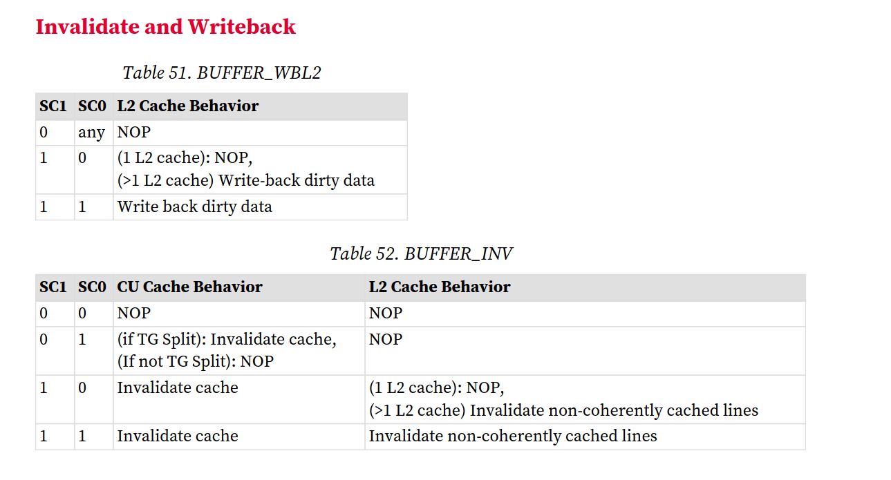
BUFFER_WBL2 pushes dirty data from private L2 slices out
to the global fabric so others can see it, while BUFFER_INV
wipes local caches to force a fresh fetch, ensuring stale data is not
read.
Hardware Counters for Pending Memory Instructions
Scope bits, cache writebacks, and cache invalidation control the visibility of memory operations—that is, where the effects of a memory access may be observed. However, visibility alone is insufficient for correct synchronization. Two additional properties are equally critical:
Completion: Knowledge of when an issued memory instruction has completed.
Ordering: The relative order in which issued memory instructions are allowed to complete with respect to one another.
To expose completion information to software, the CDNA architecture provides hardware counters that track outstanding memory operations and indicate when those operations have completed. Ordering, on the other hand, is defined through a set of architectural guarantees that constrain how different classes of memory instructions may be observed to complete.
Together, these mechanisms allow software to reason about the completion and ordering of memory operations and to construct correct synchronization protocols across compute units, XCDs, and even multiple GPUs.
Let us discuss the hardware counters first.
VM_CNT
VM_CNT tracks outstanding vector memory instructions, including global and flat memory loads and stores issued by the vector units among other things. The counter is incremented when a vector memory instruction is issued.
For load instructions, the counter is decremented once the loaded data has been written back to the destination vector registers (VGPRs).
For store instructions, the counter is decremented once the store reaches the L2 cache.
A decrement of VM_CNT therefore indicates completion of the instruction from the issuing wavefront’s perspective, not necessarily global visibility of the stored data.
LGKM_CNT
LGKM_CNT tracks outstanding scalar memory operations and shared memory (LDS) operations.
For LDS operations, the counter is incremented on issue and decremented when the load or store completes within the LDS.
Because LDS is local to a compute unit, completion of LDS operations implies immediate visibility to other wavefronts executing on the same CU.
Ordering Guarantees
Memory instructions of the same type issued by a single wavefront are guaranteed to complete in program order (note that this is not true for scalar memory reads). For example, if a wavefront issues two vector memory load instructions, the data will be written back to the destination VGPRs in the order in which the loads were issued.
However, no such ordering guarantee exists between memory instructions of different types. A wavefront issuing a vector memory load followed by a shared memory (LDS) load may observe the LDS load completing first, as the two operations are handled by different execution pipelines and tracked by independent hardware counters. Similarly, no ordering guarantees are provided across different wavefronts. If wavefront A issues a global memory load before wavefront B, the architecture does not guarantee that wavefront A will receive its data first.
S_WAITCNT
The s_waitcnt instruction allows software to explicitly wait for one or more hardware counters to fall below a specified value before continuing execution.
For example, if a wavefront issues five vector memory operations, VM_CNT will be incremented to five. Executing:
s_waitcnt vmcnt(3)
causes the wavefront to stall until VM_CNT drops to three, indicating that first two of the issued vector memory operations have completed and written their results to the VGPRs. Similarly, s_waitcnt lgkmcnt(3) waits until only LDS operations remain outstanding (assuming no scalar memory instructions were issued)
For memory writes, waiting for the counter value allows guaranteed visibility across the entire XCD because the counter is only decremented when the write has reached L2 cache. However, it does not guarantee visibility across the entire GPU/System. For that, we will need to perform a writeback from L2.
Memory Synchronization in Software
Now we have all the pieces - Memory visibility can be controlled by
the use of scope bits, cache writeback and invalidation while memory
ordering and completion can be controlled using hardware counters along
with the s_waitcnt instruction.
The compiler implements memory synchronization as requested by the software, using a combination of aforementioned instructions and memory scope bits.
At a high level, synchronization follows a producer–consumer pattern. A producing wavefront releases the results of its computation by ensuring that relevant memory operations have completed and that their effects are made visible at a specified scope. A consuming wavefront operating in the same scope subsequently acquires those results, guaranteeing that it observes the producer’s writes before performing dependent computation.
A naive way to ensure memory synchronization would be to mark the scope of every load/store to device/system level. This would ensure that every memory load/store is visible to the entire GPU/System. However, this would be massively inefficient as well, because often only the end results of a computation need to be made visible, and not the individual intermediate operations.
Release Patterns
Different instructions are used to establish visibility across different scopes. For example, consider what a wavefront A would require to make its vector memory stores visible to all the wavefronts in the same agent with multiple L2 cache configuration.
The following sequence of instructions is generated by the compiler
1 | |
First a writeback of the L2 cache is initiated which ensures that
ALL the memory operations issued are made visible to
the entire device. The buffer_wbl2 sc1=1 ensures that all
the writes (including writes that have not yet been fully
propagated through L2) are written back.
Then the s_waitcnt vmcnt(0) ensures that this writeback
is completed. Finally we have the anchor store with sc1 bit
set (device level scope) which makes it visible across the device. This
store acts like the flag which can be probed by another wavefront for
the expected value.
Acquire Pattern
On the flip side, consider what a wavefront B running on a different XCD would require to be able to read all the data written by wavefront A
The following sequence of instructions is generated by the compiler
1 | |
The first two instructions perform a system scoped load on the Flag value. Once this loaded value matches the expected value, the wavefront B invalidates its L1 and L2 cache to ensure that any following loads will skip the L1, L2 cache and reach the Infinity Cache to retrieve the latest values published by wavefront A
Similarly, there are Release-Acquire semantics for wave scope, group scope and system scope.
Detour on L2 Coherence and Snoop filters
We have seen that maintaining coherence at the L2 level requires the compiler to emit explicit writeback and invalidate instructions. However, examination of the LLVM backend for AMD CDNA-3 (gfx942) reveals some important architectural behaviors:
Local memory cache lines are automatically invalidated by writes originating from compute units associated with other L2 caches, as well as by CPU writes. This occurs due to cache probes triggered by coherent requests. Such coherent requests may arise from GPU accesses to pages with the PTE C-bit set, CPU accesses over XGMI, or PCIe transactions configured as coherent.
To ensure coherence of local memory reads across compute units with different L1 caches within the same agent, a buffer_inv sc1 instruction is required. If the agent is configured with a single L2 cache, this instruction has no effect. In configurations with multiple L2 caches, it invalidates non-local L2 cache lines.
To ensure coherence of local memory reads across compute units belonging to different agents, a buffer_inv sc0 sc1 instruction is required. In multi-L2 configurations, this instruction invalidates non-local L2 cache lines.
The following interpretation is based on code comments in the LLVM AMDGPU back end. As I could not find explicit confirmation of this behavior in the publicly available CDNA manuals, please treat them as informed speculations
Local memory here refers to memory addresses that is part of the GPU partition. The CDNA-3 architecture consists of eight XCDs distributed across four I/O dies, with a total of eight HBM stacks attached to these I/O dies. Effectively, the entire GPU can be partitoned into 1/2/4/8 GPUs with 8/4/2/1 XCDs per GPU.
The buffer_inv instructions invalidate only non-local cache lines, as invalidation of cache lines corresponding to local memory is handled automatically by hardware probes triggered through the coherence fabric.
Conclusion
GPUs deliberately expose a weak memory model that trades implicit hardware guarantees for scalability and throughput. AMD CDNA GPUs shift the responsibility of synchronization to the programmer and the compiler backend. By combining scoped memory operations with cache writeback, invalidation, and precise waiting on outstanding memory instructions, the compiler can construct efficient release–acquire synchronization patterns without sacrificing performance. Understanding these mechanisms is essential for reasoning about correctness on modern GPUs and for building compiler backends that generate synchronization which is both minimal and correct.
References
Chips and Cheese CDNA 3 architecture